Programa Prometeu per a grups d’investigació d’excel.lència, referència PROMETEO/2021/015

PROJECTE FINANCIAT PER LA CONSELLERIA D’EDUCACIÓ, INVESTIGACIÓ, CULTURA I ESPORT
PROJECT OVERVIEW
With this project we seek to support further development and consolidatation of a set of disruptive photonic technologies in which the Photonics Research labs (PRL) has produced pioneering and world-class results and which are called to play a starring role in enabling future emerging applications in communications, sensing, biomedicine, security, industry 4.0, food and agriculture, computing, transportation. These share common needs in flexibility, broadband operation, low power consumption and miniaturized footprint. The project aims to 1) further develop core knowledge in: a) programmable integrated photonics, b) Specialty SDM fibers exploiting spatial multiplexing for signal processing and sensing, c) Hybrid optical wireless-millimeter wave access networks and d) Hybrid active/passive photonic integration, 3) Train a new generation of researchers specialized in them and 3) Provide the basis for future transfer of these technologies to the industrial sector.
Photonics has been recognized by the European Unión as a Key Enabling Technolgy both under the already concluded Horizon 2020 program as well as in the new Horizon Europe scheme started in January 2021. Photonics is a pervasive technology capable of providing solutions that support a myriad of fields that span broadband communications, sensing, biomedicine, security, industry 4.0, food and agriculture, computing, transportation, etc.
To cope with the seamless list of emerging applications it has to furnish flexible solutions that provide flexible and future-proof operation, scalability, low footprint and low power consumption while increasing the speed of information processing capability. To achieve these objectives several technology approaches need to be developed and some of them, which are especially relevant, are currently in the research agenda of the Photonics Research Labs for the next years. In particular PRL has gained an outstanding and world-class reputation in the fields of RF and integrated photonics, spatial division multiplexing and photonic sensing with publications in top visibility journals, an active portfolio of patents and a relevant activity in technology transfer through the creation of 4 spin-off companies.
The ambition of this project goes beyond the current status quo and points towards the development of the full capabilities of these technologies with a view of reaching and consolidating its world-leadership during the period 2021-2030. With this aim we target our activities in the following four objectives:
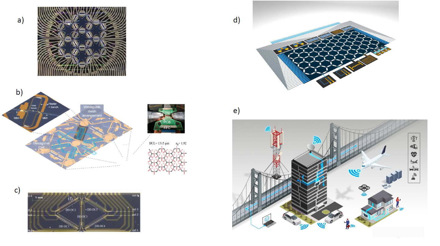
Objetive 1: Programmable Integrated Photonics
The microelectronics industry is probably one of the largest productive sectors that exist today and one of the mainstays of the 21st century economy. From the decade of the 60s to practically our days, microelectronic systems have grown uninterruptedly in capacity while fulfilling the famous Law enunciated by Gordon Moore in 1965, according to which, the number of transistors that can be integrated per unit area doubles every two years.
Unfortunately, Moore’s law is no longer fulfilled during this decade, which means an inexorable physical limitation of electronic systems for information processing and poses a technological challenge of enormous calibre for the medium and long-term future, since that the integrated microelectronic circuits are strongly implanted at present, both in the industrial and domestic sphere.
Beyond Electronics, Photonics is presented as the technological solution of future information and communication technologies. By replacing electrons with photons, photonics promises to offer both distribution and processing of data at the speed of light, providing important competitive advantages thanks to its low losses, high bandwidth (which translates into greater capacities in bit/s), immunity against electromagnetic interference, as well as flexibility and speed of reconfiguration and interconnection. All these characteristics allow, in turn, the development of new signal processing devices and even new end user applications.
One possible solution is to develop systems based on the cooperative use of both technologies, Electronics and Photonics, and which can also be integrated into a chip since both technologies are complementary. In this sense, the Integrated Photonics is a much more recent technology that is still in its early stages of development, focused primarily on the design of specific application photonic integrated circuits (ASPIC, of Application Specific Photonic Integrated Circuit). It is expected, however, that due to its similarity and parallelism with the development of the Integrated Electronics, a very important development will take place followed by a global implantation of the Programmable Integrated Photonics, and it is here, precisely, where the identified business opportunity lies.
We have identified Programmable Integrated Photonics (PIP) as a novel approach compatible and complementary to ASPICs much in the same way as FPGA programmable electronic devices (Field Programmable Gate Arrays) were to electronic Application Specific Integrated Circuits (ASICs). Furthermore, we believe that there is an unique opportunity to develop an excellency research agenda in this field that comprehensively contemplates: a) The necessary photonic / electronic hardware design by exploiting the concept of programmable integrated waveguide meshes or by developing more complex subsystems called programmable analog photonic matrices or FPPGA (Field Programmable Photonic Gate Arrays), b) The design and creation of supervision and control software for programmable photonic circuits and c) The development of software tools for the functional programming of programmable photonic circuits.
Objetive 2: Specialty SDM fibers exploiting spatial multiplexing for signal processing and sensing
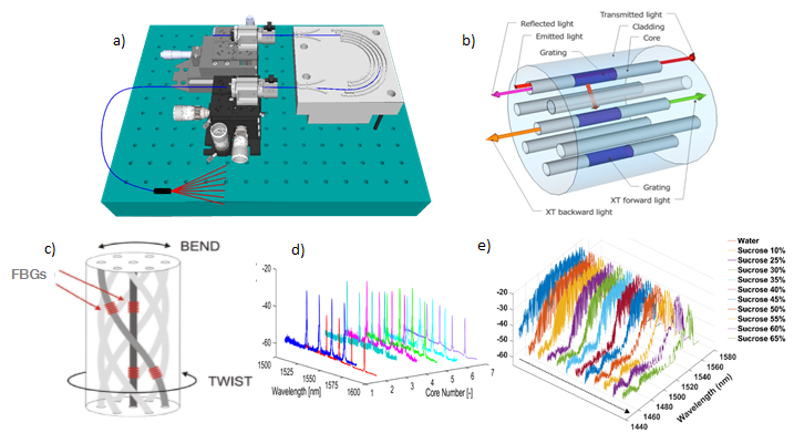
In recent years, the addition of the spatial dimension to the portfolio of optical multiplexing technologies, widely known as Space-Division Multiplexing (SDM), has been touted as a solution for the capacity bottleneck in digital communications by establishing independent light paths in one single fiber via multicore fibers (MCFs), few-mode fibers (FMFs) or a combination of both. Boosted by the benefits brought in terms of compactness, lightness and versatility, the growing interest on these novel fibers has recently opened up new avenues for research in emerging fields of application beyond long-haul digital optical communications, such as multi-parameter optical fiber sensing, radio access networks and radiofrequency (RF) signal processing. In these applications areas, SDM fibers exhibit high potential not only to deliver parallel channels (for instance, from a central office to a set of remote multi-element antennas), but also to process the microwave/optical signal or provide advanced sensing capabilities, either while it is being distributed to its final destination (fiber link) or at certain system locations (fiber-based device).
A typical fiber-wireless scenario, where emerging information and communication paradigms such as Beyond 5G or 6G or the Internet of Things demand a full integration between the optical fiber network and the wireless network while keeping the requirements in terms of high capacity, parallel connectivity and system flexibility. To address these demands, with this project we aim at pioneering and developing innovative optical technologies based on specialty SDM fibers to revolutionize the future display of broadband fibers-wireless communication scenarios.
More specifically, our general goal is to exploit the inherent parallelism of multicore fibers, few-mode fibers and combination of both to implement a variety of signal processing and multiparameter sensing applications featuring unique properties beyond the state of the art in terms of compactness, lightness, system stability, power efficiency, versatility and record bandwidth.
Objetive 3: Hybrid optical wireless-millimeter wave access networks
The continuous growth of the number of smartphones, wearables, tablets or Internet of Things (IoT) devices, and the emerging of the new multimedia services, such as cloud access, 4K/8K high-definition video, augmented virtual reality, online gaming or social networking exceed the capabilities of the current mobile network communications. As expected, there will be 5.3 billion total internet users (66% of global population) by 2023, the number of mobile devices will increase up to 13.1 billion in 2023 and 1.4 billion of these will make use of 5G communications. The evolution of the legacy mobile communications up to 5G and beyond will provide downlink experience user of 100 Mb/s, 30 bps/Hz spectral efficiency, latency lower than 1 ms, connection density of 1,000,000 device/km2 and highly efficient power consumption.
Due to congestion of lower microwave bands employed in conventional cellular services, millimeter wave (mmW) band (30-300 GHz) was proposed for 5G mobile communications with large spectral availability and delivered throughput. Therefore, mmW radio is the new interface for mobile users in 5G. Of course, this frequency range leads to small-cell networks with high frequency reuse and minimal interference between adjacent cells. During the recent years, there has been much research on how to generate and transmit Ka, W and also E-bands radio-over fiber systems.
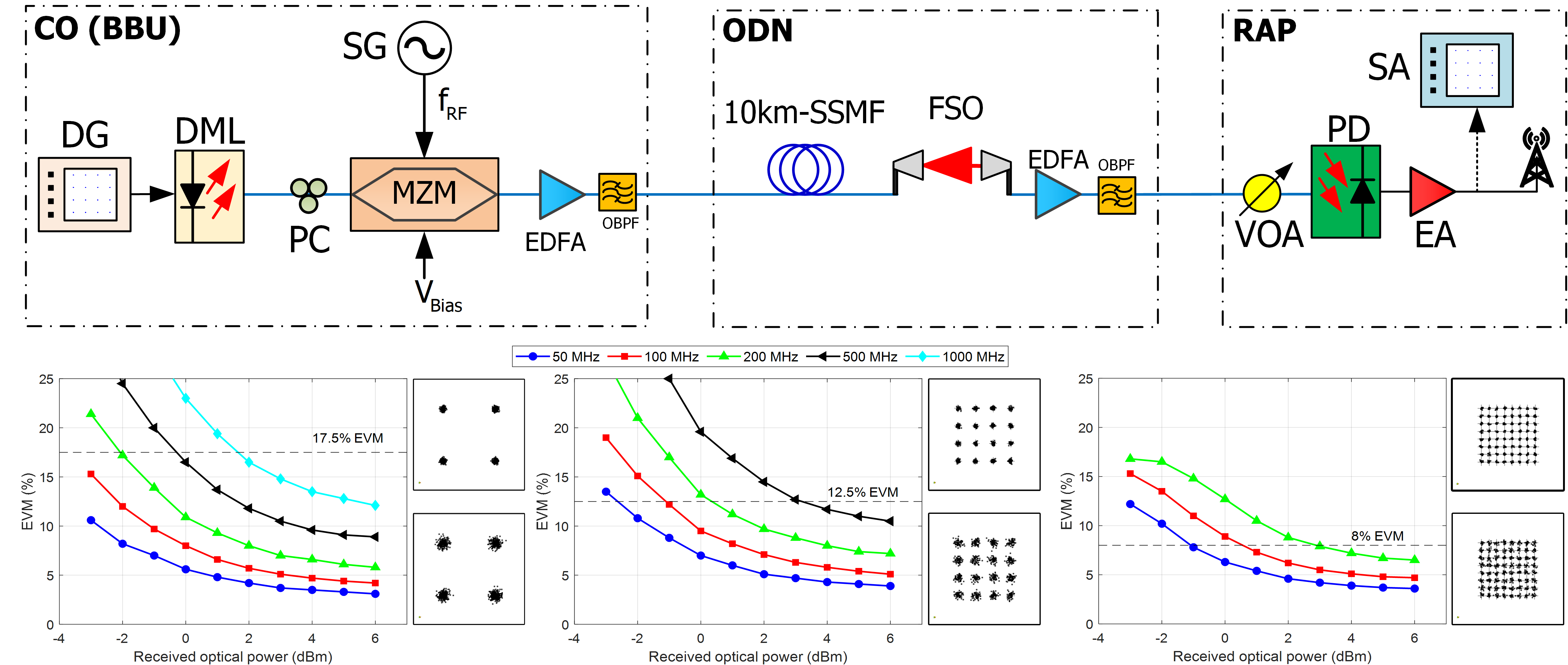
Photonic generation of mmW signals offers low phase noise and frequency tunability in addition to the use of electronics components with reduced bandwidth. Although different approaches based on dual-mode sources, mode-locked lasers, pulsed lasers or nonlinear effects amongst others have been previously demonstrated, external Mach-Zehnder modulators (MZM) can be considered as the most popular approach due to high quality and efficient mmW signal generation. Depending on the bias point of the external modulator, optical single sideband (SS), double sideband (DSB) and carrier suppression (CS) techniques can be employed to provide frequency multiplying with a factor from 2 up to 12.
The preferred architecture for 5G networks is centralized cloud-radio access network (C-RAN), which hosts the baseband units (BBUs) at the central office (CO) separated from the analog remote radio heads (RRH) or radio access points (RAP). This leads to the fronthaul segment connecting the RAPs with the centralized BBU pool. A backhaul segment is also defined between the BBUs and the gateway interface to the transport network. Therefore, RAPs are simplified since medium access control (MAC) layer functions, digital to analog and analog to digital conversion (DAC/ADC), radio frequency (RF) frontends and baseband processing are held in the BBUs located at the CO. The BBU pool can include an array of directly modulated lasers (DMLs) emitting at different wavelengths which are multiplexed for downlink transmission . However, installation of optical fiber (OF) is sometimes limited due to the high cost, especially in multidense environment or because of the restrictions on cable installation. Free-space Optics (FSO) technology, which is able to offer a large bandwidth over flexible and cost-effective free-space links, can be an effective alternative for mobile fronthaul. Figure WO_1 shows recent results on the use of DMLs for effective transmission, of M-QAM signals with different bandwidths at 40 GHz over hybrid links. Of course, none of these technologies is a stand-alone solution for cost-effective, highly scalable and high-capacity wired and wireless access in 5G networks. While OF is still the preferred choice for upper-tier connections, mmW RF and FSO are more adequate in general for the high-density small cells. At the hotspot site, after channel demultiplexing, the optical receiver in each RAP performs the optoelectronic conversion and further amplification. The variety of access segments forming the global telecommunication network includes indoor mmW small cells access as well as fiber broadband access in residential areas and also outdoor emerging small-cell C-RAN systems.
Indoor access requires massive MIMO with a large number of antenna elements, and also large phased arrays as the antenna remote units providing even multibeam solutions. However, this is very challenging from what is available today, especially due to the expensive components in the market. Although the capital and operating expenditures (CAPEX and OPEX, respectively) reduction is a benefit in cloud-radio access network (C-RAN) networks, the availability and costs of the optical infrastructure becomes critical, especially in the small-cell environment.
In terms of network architecture, the use of massively distributed antennas (massive DAS) would bring radio access points (RAPs) closer to users and allow for extremely high spectrum reuse and connection densities in future wireless systems. Due to the short distance between RAP and users, radio access links are only a very small portion of the entire system. The power consumption and complexity of optical links could easily dominate their wireless counterparts. Therefore, it is essential to quantitatively identify the impact of optical fronthaul links across the network, thus achieving optimal designs of these networks when considering the complex interactions between the wireless and optical domains.
The optimum design of hybrid optical wireless-millimeter wave access networks must consider the complex interactions between the optical and wireless domains. Massive number of spatially distributed RAPs in C-RANs must rely on advanced fronthaul techniques to achieve coordination and cooperation across geographically distributed antennas, such that all users in the network can enjoy uniformly good services regardless of their actual location.
Noise and distortions in fiber and free space optics links are accumulated in the optical domain and propagated to the wireless domain, and this will have significant impact on the design and performance of the overall system. As a result, optical fronthauls must be designed by considering the characteristics of the wireless links and vice versa. One aspect that can directly benefit from cross-domain design is the development of beamforming, which is an essential component for all massively DAS. The spatially distributed RAPs form a distributed antenna array. An approach based on the combination of digital and optical techniques for beamforming will be implemented to outperform existing electrical beamforming schemes for future generation networks, especially for wideband applications, due to the linear phase with true-time delay beamforming in the optical domain.Thus, beamforming can be employed by the cooperating RAPs to steer and focus the signal to the user towards higher performance and more efficient networks and also allow multibeam operation in mmW advanced designs.
All of these beamforming techniques require precise synchronization among all cooperating RAPs or antennas since a small error in synchronization may cause corruption of the beam pattern, resulting in significant performance losses. However, the synchronization modules increase the cost, complexity, and power consumption of RAPs, and artificial intelligence will be also considered for smart control of massive resources.
Therefore, this Project will make a major breakthrough towards the realization of high performance, cost effective and flexible hybrid full duplex access networks based on fiber, FSO and radio access links operating in the millimeter wave band for future 6G mobile communications.
Objetive 4: Hybrid III-V / silicon nitride photonic integration platform
Photonics is the discipline that deals with light applications across the entire wavelength spectrum, from visible (VIS, l = 0.4-0.7 µm) through near infrared (NIR, l = 0.7-3 µm) to the mid infrared, (MIR, l = 3-12 µm). Although the applications of light in each of these bands are multiple, in general the VIS range has been used for bio-photonics (VIS radiation is non-ionizing for biological samples), the NIR for telecommunications (silica optical fiber presents transmission windows from 0.9 to 1.7 µm) and the MIR for sensors (the molecules have unique spectral signature in this range of l). In all of them, a light emitter, a combination of passive components (e.g., that allow and enhance the interaction of light with the medium in the case of a sensor application), the light transmission medium, and a light detector, which collects the signals after passing through the passive components and the medium, are required.
Many of the applications build these systems with discrete optical components, (e.g., in transmission systems, a laser usually with modulator, using fiber optics as medium, and then terminated in a detector), but more and more many applications make use of integrated photonics, where the light is confined in a multilayer structure of different materials, properly patterned. This is the analogous version to integrated electronic circuits, that take a prominent place in our daily life already for some decades: televisions, computers, mobile phones, among others.
Although in the micro-electronics there is a common core technology based on Silicon, in integrated photonics, whose current state is similar to that of micro-electronics three decades ago, there are several of them, with different features depending on the materials with which they are constructed. Hence, they allow to cover one or several of the aforementioned wavelength ranges, VIS, NIR and MIR. Expressed in very general terms, the choice of the materials with which the waveguides are constructed, determines the range of wavelengths (where the material is transparent) and therefore, the applications a PIC can serve. Silicon nitride (Si3N4) is highlighted as a material whose range of transparency covers VIS, NIR and MIR. However, to date it has been used in microstructures in which it is surrounded by silicon oxide (SiO2). But SiO2 is only transparent up to approximately 3.4-3.7 µm of wavelength, thereby limiting the range of usable wavelengths, and therefore the applications of this Si3N4/SiO2 technology.
The Existing PIC technology platforms are limited to a given wavelength range. Therefore, the first technological challenge in this project is to investigate and develop a broadband photonic integration passive platform, based on the micro-manufacturing techniques and design processes of associated PICs using Si3N4 to cover VIS, NIR and MIR. Besides, Si3N4 is passive material, that is, without the ability to generate and detect light, is a key feature of semiconductors so there is the need to combine Si3N4 with them for fully active-passive operating platform.
On-going research in the field pursues the heterogeneous and/or hybrid integration of III-V semiconductor with silicon / silicon nitride passive platforms, and market reports forecast a growth of industrial activity in this area as well. Consequently, the second technological challenge in this project is to develop the design and transfer processes of active material (multilayer semiconductor III-Vs), onto Si3N4 broadband technology, resulting in a hybrid active-passive platform of Si3N4 / III-V.
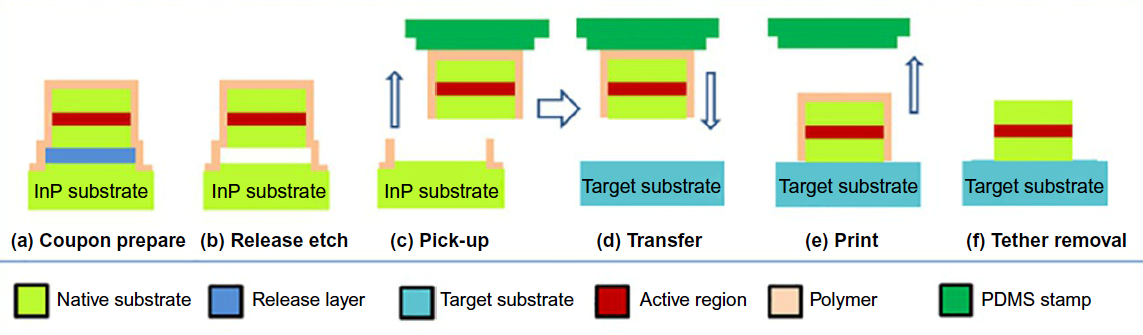
So far, the Si3N4 platform developments carried out in the past years by our group and in cooperation with the main actors in the ecosystem, do only address purely passive operations. Truly active optical functions, such as the generation and detection of light, are highly incompatible (at least from a power efficiency aspect) with these silicon-based PIC platforms. The hybrid integration of lasers or optical amplifiers onto passive photonic circuitry has been usually addressed either by i) coupling the radiated beams of a III-V device to a Si/SiNx photonics (using grating or edge couplers) or ii) by bonding III-V wafers onto Si/SiNx (evanescently coupled devices). Both techniques are suitable, however they present several short-comings, the most relevant is the poor utilization of (costly) III-V material. They do also require precise alignment among the actives and the host substrate. On the other hand, the heterogeneous integration aims at growing III-V materials directly on top of Si-based technologies, and later processing the so-formed heterogeneous layer-stack within the same micro-fabrication. In summary, Bowers advocates in for the epitaxial growth of III-V on silicon. The main technical and economic reasons to do so is that the resulting process will be employed for a given reduced set of applications (wavelength range constrained) and for a mass market (to pay back the costs of developing this highly challenging technological process). As introduced above, in this research project we are pursuing a different approach: a broad band photonic technology platform. This is in contrast with heterogeneous integration described above: the process has not to be constrained in wavelength. Furthermore, the economics of the pursued processes to bring actives onto SiNx will need to suit niche, rather than mass, applications. Therefore, a hybrid integration approach is proposed. Besides the optical coupling and bonding hybridization techniques mentioned in the previous paragraph, Roelkens and co-workers have demonstrated the use of micro-transfer printing [PIC_10] for hybrid integration of III-V’s and silicon photonics. The native substrate hosts the ‘coupons’ of active layers on top of a sacrificial release layer and surrounded by tethers. Next the release layer is under-etched, and the coupon is released with a PDMS stamp that is pulled fast to break the tethers. The coupon is then transferred to the target substrate and stamped (directly or with an intermediate polymer layer) by slowly pulling off the PDMS stamp.
The group is addressing a hot scientific topic, that has high potential for transfer to the industry. Thus, the group is procuring ahead of time with the capabilities to do so. Hence, and with the support of the key player in micro-transfer printing technologies X-Celeprint, the group has an active project granted (GVA/IDIFEDER20/029) for infrastructure acquisition in the pilot line UPVfab (www.fab.upv.es). The project funds are for the procurement of one µTP tool by 2021. Hence, we plan part of 2021 in the present project to define the process flows of the Si3N4 technology and III-V technologies, and kick-off their development. Hybrid integration per se would then happen from 2022 onward.
Disruptive Photonics Technologies Team


Beatriz Ortega

Salvador Sales
Ivana Gasulla

Daniel Pastor

Pascual Muñoz