- They report the first reconfigurable photonic chip integrated in silicon designed to perform different functionalities within a common architecture.
- The work has been published by Nature Communications. This versatile device can be potentially employed in mobile communications, the Internet of Things, quantum communications, surveillance, defence and avionic systems.
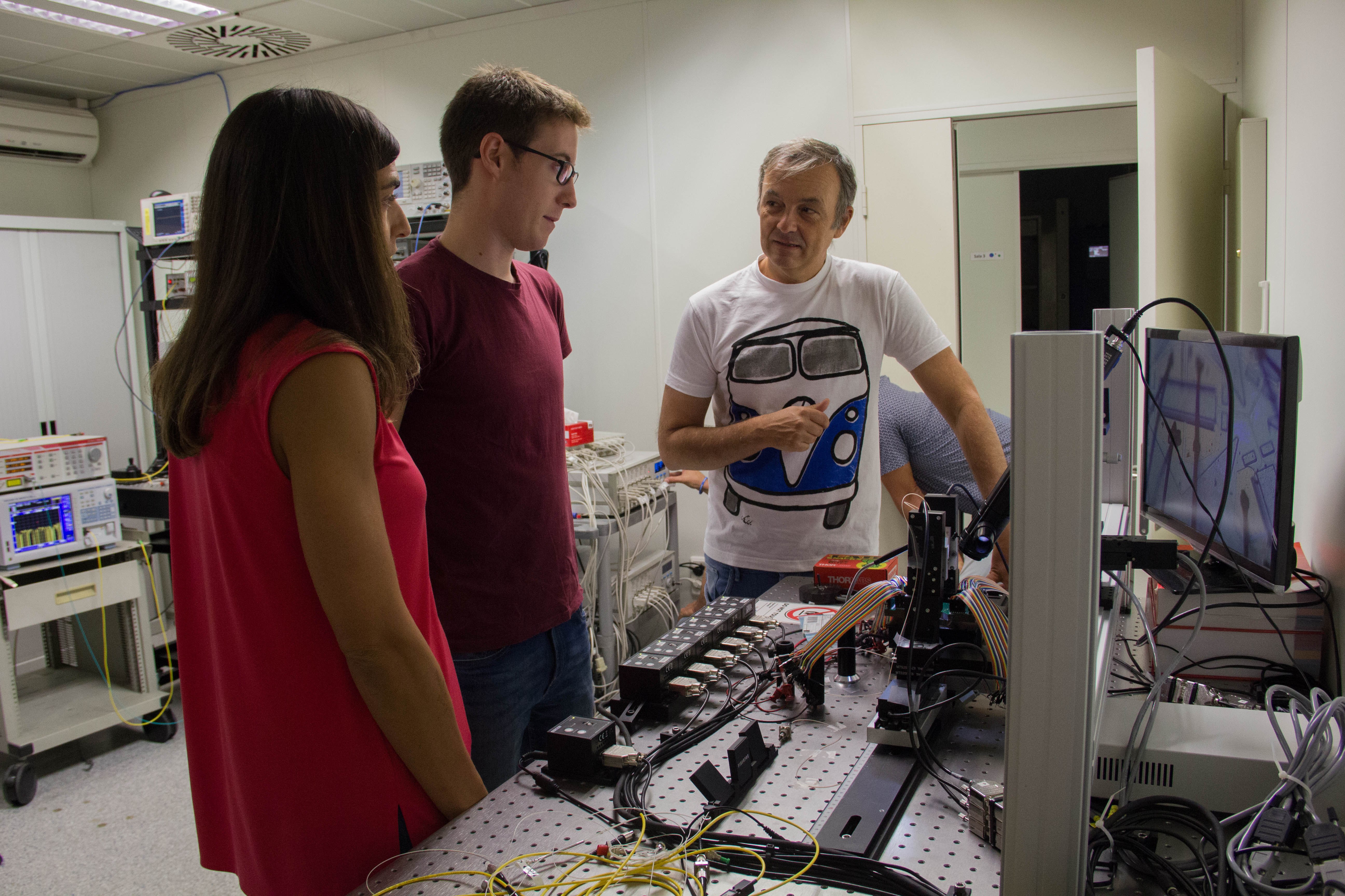
Researchers from the Photonic Research Labs (PRL) at the Universitat Politècnica de València and from the Optoelectronics Research Centre at the University of Southampton have developed the first photonic integrated chip that enables multiple functionalities by employing a single common architecture. Its behaviour is similar to the one performed in electronic microprocessors, where a common hardware is programmed to perform a desired operation. Potential applications in mobile communications and self-driven cars will benefit from the flexible and versatile performance of this device.
“By programming the internal connections of a single chip architecture, we can configure the chip to perform different functionalities.” highlights José Capmany, iTEAM researcher and coordinator of the work. Their impressive results have been published in Nature Communications.
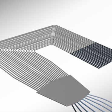
The chip architecture relies on a honeycomb waveguide mesh implemented by properly cascading tunable light couplers developed by Daniel Pérez within the framework of his Ph.D. Thesis, under the supervision of José Capmany and Ivana Gasulla. The independent basic coupler configuration allows the definition of flexible interconnection schemes as well as the definition of different optical signal processing circuits.
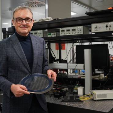
“The main advantage of this approach is that the physical hardware architecture is manufactured independently from the targeted functionality to be performed, which reduces the price of design, fabrication and testing iterations”, said Ivana Gasulla. The chip, once designed and tested, enables the configuration of more than 100 photonic signal processing circuits. In this work, around 30 configurations have been demonstrated, resulting, anyway, in the highest number reported to date as Daniel Pérez points out.
“The approach followed by this work represents a paradigm shift in the field of integrated photonics, from application specific photonic integrated circuits to generic purpose and programmable devices, in the same way as the one experienced successfully by the electronic field in the 80’s”, adds José Capmany, principal investigator of the UMWP-CHIP ERC Advanced Grant financed by the European Research Council.
Applications
Regarding its application fields, the researchers highlight self-driven cars and mobile communications, quantum computing, distributed sensors, sensing monitoring, the Internet of Things, defence, avionics and surveillance systems. In general, any field susceptible from the requirement of optical or radiofrequency signal processing.
“The small footprint of the chip enables its placement in systems with reduced size requirements, performing as the interface between radio and fibre segments. For example, in self-driven cars and avionics, it could be employed to interface the radiofrequency sensors and LIDAR from the outer part of the craft to the inner fibre optic bus”, concludes Ivana Gasulla.
Reference:
Daniel Pérez, Ivana Gasulla, Lee Crudgington, David J. Thomson, Ali Z. Khokhar, Ke Li, Wei Cao, Goran Z. Mashanovich & José Capmany. Multipurpose silicon photonics signal processor core. Nature Communications 8. doi:10.1038/s41467-017-00714-1
Read that news item on the UPV website
1 Comment
Comments are closed.